Manufacturing semiconductors involves the combination of principles involving physics, chemistry, electricity, electronics, metallurgy, and more. Silicon is widely used in this industry as it is the element most suitable for patterning integrated components (circuits) like transistors; main reason is its characteristic to readily form an oxide coating around said components.
Silicon (Si) is the second most common element in the Earth’s crust and is usually found in its silicon dioxide (SiO2) state also-known-as silica sand. To achieve the metallurgical grade Silicon however, it needs to be freed from this compound via electric arc furnace through carbon reduction:
The resulting silicon grade is then possible for use in steel transformer but it is not pure enough for the semiconductor industry. To remedy this, silicon is converted to its chloride (SiCl4 or SiHCl3) form and subsequently subjected to fractional distillation process. To further yield ultrapure silicon two different approaches can be taken:
- reduction of the sample by ultrapure zinc or magnesium; or
- thermal decomposition on a hot polycrystalline silicon rod heater by hydrogen.
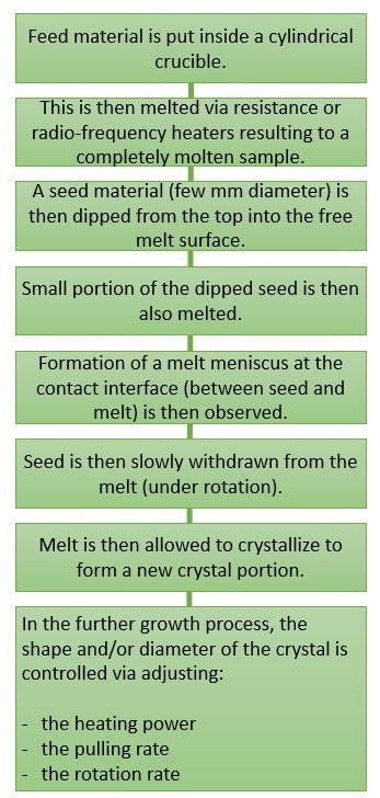
Figure 1. Steps of the Czochralski method.
Cz method allows the growth of dislocation wherein free silicon crystals (300 mm diameter) are produced for industrial use. During crystal growth via Cz, time dependent electromagnetic fields control the flow in electrically conducting melts for the manufacture of semiconductors.
On the other-hand, if the material that will be subjected to growth has components with a high partial pressure at its melting point, a modified Cz method can be done which is known as the Liquid Encapsulated Czochralski (LEC) method.
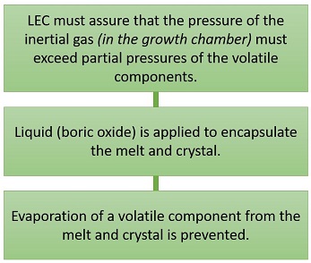
Figure 2. Liquid Encapsulated Czochralski (LEC) method..
LEC method is used for growing semiconductor compounds such as: GaAs, GaP, InP, PbSe, PbTe.
In this day and age the advancement of semiconductors for nanotechnology has increased, making it possible to achieve the purity of silicon used for its production, as high as 99.999999999% !
References:
- Anon. (2020). Semiconductor Manufacturing Techniques | Solid-state Device Theory | Electronics Textbook. Retrieved 13 December 2020, from https://www.allaboutcircuits.com/textbook/semiconductors/chpt-2/semiconductor-manufacturing-techniques/
- ANSI. (2020). Other Semiconductor Standards. Retrieved 13 December 2020, from https://webstore.ansi.org/industry/semiconductors/other
- Clean Room & ISO Classifications. (2020). Retrieved 13 December 2020, from https://www.americancleanrooms.com/cleanroom-classifications/
- Czochralski Process - an overview | ScienceDirect Topics. (2020). Retrieved 13 December 2020, from https://www.sciencedirect.com/topics/chemistry/czochralski-process
Recommended Products

.webp)
 Thailand_1.webp)